| . |  |
. |
|
|
. |
by Staff Writers Champaign, IL (SPX) Jul 26, 2011
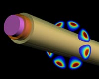
In an advance that could open new avenues for solar cells, lasers, metamaterials and more, researchers at the University of Illinois have demonstrated the first optoelectronically active 3-D photonic crystal. "We've discovered a way to change the three-dimensional structure of a well-established semiconductor material to enable new optical properties while maintaining its very attractive electrical properties," said Paul Braun, a professor of materials science and engineering and of chemistry who led the research effort. The team published its advance in the journal Nature Materials. Photonic crystals are materials that can control or manipulate light in unexpected ways thanks to their unique physical structures. Photonic crystals can induce unusual phenomena and affect photon behavior in ways that traditional optical materials and devices can't. They are popular materials of study for applications in lasers, solar energy, LEDs, metamaterials and more. However, previous attempts at making 3-D photonic crystals have resulted in devices that are only optically active that is, they can direct light but not electronically active, so they can't turn electricity to light or vice versa. The Illinois team's photonic crystal has both properties. "With our approach to fabricating photonic crystals, there's a lot of potential to optimize electronic and optical properties simultaneously," said Erik Nelson, a former graduate student in Braun's lab who now is a postdoctoral researcher at Harvard University. "It gives you the opportunity to control light in ways that are very unique to control the way it's emitted and absorbed or how it propagates." To create a 3-D photonic crystal that is both electronically and optically active, the researchers started with a template of tiny spheres packed together. Then, they deposit gallium arsenide (GaAs), a widely used semiconductor, through the template, filling in the gaps between the spheres. The GaAs grows as a single crystal from the bottom up, a process called epitaxy. Epitaxy is common in industry to create flat, two-dimensional films of single-crystal semiconductors, but Braun's group developed a way to apply it to an intricate three-dimensional structure. "The key discovery here was that we grew single-crystal semiconductor through this complex template," said Braun, who also is affiliated with the Beckman Institute for Advanced Science and Technology and with the Frederick Seitz Materials Research Laboratory at Illinois. "Gallium arsenide wants to grow as a film on the substrate from the bottom up, but it runs into the template and goes around it. It's almost as though the template is filling up with water. As long as you keep growing GaAs, it keeps filling the template from the bottom up until you reach the top surface." The epitaxial approach eliminates many of the defects introduced by top-down fabrication methods, a popular pathway for creating 3-D photonic structures. Another advantage is the ease of creating layered heterostructures. For example, a quantum well layer could be introduced into the photonic crystal by partially filling the template with GaAs and then briefly switching the vapor stream to another material. Once the template is full, the researchers remove the spheres, leaving a complex, porous 3-D structure of single-crystal semiconductor. Then they coat the entire structure with a very thin layer of a semiconductor with a wider bandgap to improve performance and prevent surface recombination. To test their technique, the group built a 3-D photonic crystal LED the first such working device. Now, Braun's group is working to optimize the structure for specific applications. The LED demonstrates that the concept produces functional devices, but by tweaking the structure or using other semiconductor materials, researchers can improve solar collection or target specific wavelengths for metamaterials applications or low-threshold lasers. "From this point on, it's a matter of changing the device geometry to achieve whatever properties you want," Nelson said. It really opens up a whole new area of research into extremely efficient or novel energy devices. The U.S. Department of Energy and the Army Research Office supported this work. Other Illinois faculty involved in the project are electrical and computer engineering professors James Coleman and Xiuling Li, and materials science and engineering professor John Rogers. The paper, Epitaxial Growth of Three-Dimensionally Architectured Optoelectronic Devices, is available from the News Bureau.
|
. |
|
| The content herein, unless otherwise known to be public domain, are Copyright 1995-2011 - Space Media Network. AFP and UPI Wire Stories are copyright Agence France-Presse and United Press International. ESA Portal Reports are copyright European Space Agency. All NASA sourced material is public domain. Additional copyrights may apply in whole or part to other bona fide parties. Advertising does not imply endorsement,agreement or approval of any opinions, statements or information provided by Space Media Network on any Web page published or hosted by Space Media Network. Privacy Statement |

 del.icio.us
 Digg
Digg Reddit
 Google