 |
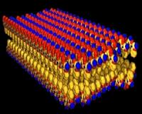
Los Angeles CA (SPX) Feb 21, 2011 In recent years, topological insulators have become one of the hottest topics in physics. These new materials act as both insulators and conductors, with their interior preventing the flow of electrical currents while their edges or surfaces allow the movement of a charge. Perhaps most importantly, the surfaces of topological insulators enable the transport of spin-polarized electrons while preventing the "scattering" typically associated with power consumption, in which electrons deviate from their trajectory, resulting in dissipation. Because of such characteristics, these materials hold great potential for use in future transistors, memory devices and magnetic sensors that are highly energy efficient and require less power. In a study published Feb. 13 in Nature Nanotechnology, researchers from UCLA's Henry Samueli School of Engineering and Applied Science and from the materials division of Australia's University of Queensland show the promise of surface-conduction channels in topological insulator nanoribbons made of bismuth telluride and demonstrate that surface states in these nanoribbons are "tunable" - able to be turned on and off depending on the position of the Fermi level. "Our finding enables a variety of opportunities in building potential new-generation, low-dissipation nanoelectronic and spintronic devices, from magnetic sensing to storage," said Kang L. Wang, the Raytheon Professor of Electrical Engineering at UCLA Engineering, whose team carried out the research. Bismuth telluride is well known as a thermoelectric material and has also been predicted to be a three-dimensional topological insulator with robust and unique surface states. Recent experiments with bismuth telluride bulk materials have also suggested two-dimensional conduction channels originating from the surface states. But it has been a great challenge to modify surface conduction, because of dominant bulk contribution due to impurities and thermal excitations in such small-band-gap semiconductors. The development of topological insulator nanoribbons has helped. With their large surface-to-volume ratios, these nanoribbons significantly enhance surface conditions and enable surface manipulation by external means. Wang and his team used thin bismuth telluride nanoribbons as conducting channels in field-effect transistor structures. These rely on an electric field to control the Fermi level and hence the conductivity of a channel. The researchers were able to demonstrate for the first time the possibility of controlling surface states in topological insulator nanostructures. "We have demonstrated a clear surface conduction by partially removing the bulk conduction using an external electric field," said Faxian Xiu, a UCLA staff research associate and lead author of the study. "By properly tuning the gate voltage, very high surface conduction was achieved, up to 51 percent, which represents the highest values in topological insulators." "This research is very exciting because of the possibility to build nanodevices with a novel operating principle," said Wang, who is also associate director of the California NanoSystems Institute (CNSI) at UCLA. "Very similar to the development of graphene, the topological insulators could be made into high-speed transistors and ultra-high-sensitivity sensors." The new findings shed light on the controllability of the surface spin states in topological insulator nanoribbons and demonstrate significant progress toward high surface electric conditions for practical device applications. The next step for Wang's team is to produce high-speed devices based on their discovery. "The ideal scenario is to achieve 100 percent surface conduction with a complete insulating state in the bulk," Xiu said. "Based on the current work, we are targeting high-performance transistors with power consumption that is much less than the conventional complementary metal-oxide semiconductors (CMOS) technology used typically in today's electronics." Study collaborators Jin Zou, a professor of materials engineering at the University of Queensland; Yong Wang, a Queensland International Fellow; and Zou's team at the division of materials at the University of Queensland contributed significantly to this work. A portion of the research was also done in Alexandros Shailos' lab at UCLA.
Share This Article With Planet Earth
Related Links University of California - Los Angeles Nano Technology News From SpaceMart.com Computer Chip Architecture, Technology and Manufacture
 New Nanomaterials Unlock New Electronic And Energy Technologies
Dublin, Ireland (SPX) Feb 07, 2011 A new way of splitting layered materials to give atom thin "nanosheets" has been discovered. This has led to a range of novel two-dimensional nanomaterials with chemical and electronic properties that have the potential to enable new electronic and energy storage technologies. The collaborative international research led by the Centre for Research on Adaptive Nanostructures and Nanodevices ... read more |
|
| The content herein, unless otherwise known to be public domain, are Copyright 1995-2010 - SpaceDaily. AFP and UPI Wire Stories are copyright Agence France-Presse and United Press International. ESA Portal Reports are copyright European Space Agency. All NASA sourced material is public domain. Additional copyrights may apply in whole or part to other bona fide parties. Advertising does not imply endorsement,agreement or approval of any opinions, statements or information provided by SpaceDaily on any Web page published or hosted by SpaceDaily. Privacy Statement |


 del.icio.us
 Digg
Digg Reddit
 YahooMyWeb
 Google