 |
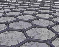
Manchester UK (SPX) Mar 05, 2007 Researchers have used the world's thinnest material to create the world's smallest transistor - a breakthrough that could spark the development of a new type of super-fast computer chip. Professor Andre Geim and Dr Kostya Novoselov from The School of Physics and Astronomy at The University of Manchester, reveal details of transistors that are only one atom thick and less than 50 atoms wide, in the March issue of Nature Materials. They believe this innovation will allow the rapid miniaturisation of electronics to continue when the current silicon-based technology runs out of steam. In recent decades, manufacturers have crammed more and more components onto integrated circuits. As a result, the number of transistors and the power of these circuits has roughly doubled every two years. This has become known as Moore's Law. But the speed of cramming is now noticeably decreasing, and further miniaturisation of electronics is to experience its most fundamental challenge in the next ten to 20 years, according to the semiconductor industry roadmap. Two years ago, Professor Andre Geim and his colleagues discovered a new class of materials that can be viewed as individual atomic planes pulled out of bulk crystals. These one-atom-thick materials and particularly graphene - a gauze of carbon atoms resembling a chicken wire - have rapidly become one of the hottest topics in physics. The first graphene-based transistor was reported by The University of Manchester team at the same time as the discovery of graphene, and other groups have recently reproduced the result (1). But these graphene transistors were very 'leaky' (2), which has limited possible applications and ruled out important ones, such as their use in computer chips and other electronic circuits with a high density of transistors. Now the Manchester team has found an elegant way around the problem and made graphene-based transistors suitable for use in future computer chips. Professor Geim and colleagues have shown for the first time that graphene remains highly stable and conductive even when it is cut into strips of only a few nanometres (3) wide. All other known materials - including silicon - oxidise, decompose and become unstable at sizes tens times larger. This poor stability of these materials has been the fundamental barrier to their use in future electronic devices - and this has threatened to limit the future development of microelectronics. "We have made ribbons only a few nanometres wide and cannot rule out the possibility of confining graphene even further - down to maybe a single ring of carbon atoms," says Professor Geim. The research team suggests that future electronic circuits can be carved out of a single graphene sheet. Such circuits would include the central element or 'quantum dot', semitransparent barriers to control movements of individual electrons, interconnects and logic gates - all made entirely of graphene. Geim's team have proved this idea by making a number of single-electron-transistor devices that work under ambient conditions and show a high-quality transistor action. "At the present time no technology can cut individual elements with nanometre precision. We have to rely on chance by narrowing our ribbons to a few nanometres in width," says Dr Leonid Ponomarenko, who is leading this research at The University of Manchester. "Some of them were too wide and did not work properly whereas others were over-cut and broken." But Dr Ponomarenko is optimistic that this proof-of-concept technique can be scaled up. "To make transistors at the true-nanometre scale is exactly the same challenge that modern silicon-based technology is facing now. The technology has managed to progress steadily from millimetre-sized transistors to current microprocessors with individual elements down to tens nanometres in size. "The next logical step is true nanometre-sized circuits and this is where graphene can come into play because it remains stable - unlike silicon or other materials - even at these dimensions." Professor Geim does not expect that graphene-based circuits will come of age before 2025. Until then, silicon technology should remain dominant. But he believes graphene is probably the only viable approach after the silicon era comes to an end. "This material combines many enticing features from other technologies that have been considered as alternatives to the silicon-based technology. "Graphene combines most exciting features from carbon-nanotube, single-electron and molecular electronics, all in one." Previous releases on graphene for background: - Discovery of Two-Dimensional Fabric Denotes Dawn of New Materials Era here - One-atom-thick materials promise a 'new industrial revolution' here - Einstein's relativity theory proven with the 'lead' of a pencil here Related Links Manchester School of Physics and Astronomy Powering The World in the 21st Century at Energy-Daily.com Our Polluted World and Cleaning It Up China News From SinoDaily.com Global Trade News The Economy All About Solar Energy at SolarDaily.com Civil Nuclear Energy Science, Technology and News Computer Chip Architecture, Technology and Manufacture Nano Technology News From SpaceMart.com
 Bangalore (AFP) India, Feb 23, 2007
India is to offer microchip makers incentives including tax breaks and subsidies to set up factories, a policy the industry welcomed Friday to lure global giants and turn the country into a chip manufacturing hub. "The policy will go a long way in making India an attractive destination for global semiconductor and hi-tech companies," said Poornima Shenoy, president of the Bangalore-based India Semiconductor Association. |
|
| The content herein, unless otherwise known to be public domain, are Copyright Space.TV Corporation. AFP and UPI Wire Stories are copyright Agence France-Presse and United Press International. ESA Portal Reports are copyright European Space Agency. All NASA sourced material is public domain. Additional copyrights may apply in whole or part to other bona fide parties. Advertising does not imply endorsement, agreement or approval of any opinions, statements or information provided by Space.TV Corp on any Web page published or hosted by Space.TV Corp. Privacy Statement |