 |
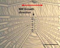
Washington DC (SPX) Oct 29, 2007 In the growing catalog of nanoscale technologies, nanowires-tiny rows of conductor or semiconductor atoms-have attracted a great deal of interest for their potential to build unique atomic-scale electronics. But before you can buy some at your local Nano Depot, manufacturers will need efficient, reliable methods to build them in quantity. Researchers at the National Institute of Standards and Technology (NIST) believe they have one solution-a technique that allows them to selectively grow nanowires on sapphire wafers in specific positions and orientations accurately enough to attach contacts and layer other circuit elements, all with conventional lithography techniques. Despite their name, nanowires are more than just electrical connectors. Researchers have used nanowires to create transistors like those used in memory devices and prototype sensors for gases or biomolecules. However working with objects only tens of nanometers wide is challenging. A common approach in the lab is to grow nanowires like blades of grass on a suitable substrate, mow them off and mix them in a fluid to transfer them to a test surface, using some method to give them a preferred orientation. When the carrier fluid dries, the nanowires are left behind like tumbled jackstraws. Using scanning probe microscopy or similar tools, researchers hunt around for a convenient, isolated nanowire to work on, or place electrical contacts without knowing the exact positions of the nanowires. It's not a technique suitable for mass production. Building on earlier work to grow nanowires horizontally on the surface of wafers (see "Gold Nano Anchors Put Nanowires in Their Place"), NIST researchers used conventional semiconductor manufacturing techniques to deposit small amounts of gold in precise locations on a sapphire wafer. In a high-temperature process, the gold deposits bead up into nanodroplets that act as nucleation points for crystals of zinc oxide, a semiconductor. A slight mismatch in the crystal structures of zinc oxide and sapphire induces the semiconductor to grow as a narrow nanowire in one particular direction across the wafer. Because the starting points and the growth direction are both well known, it is relatively straightforward to add electrical contacts and other features with additional lithography steps. As proof of concept, the NIST researchers have used this procedure to create more than 600 nanowire-based transistors, a circuit element commonly used in digital memory chips, in a single process. In the prototype process, they report, the nanowires typical grew in small bunches of up to eight wires at a time, but finer control over the size of the initial gold deposits should make it possible to select the number of wires in each position. The technique, they say, should allow industrial-scale production of nanowire-based devices. Related Links National Institute of Standards and Technology (NIST) Nano Technology News From SpaceMart.com Computer Chip Architecture, Technology and Manufacture
 Troy NY (SPX) Oct 24, 2007
Taking advantage of the material's unique electrical and mechanical properties, researchers repeatedly squeezed a 3-millimeter nanotube block and discovered it was highly suitable for potential applications as a pressure sensor. No matter how many times or how hard they squeezed the block, it exhibited a constant, linear relationship between how much force was applied and electrical resistance. |
|
| The content herein, unless otherwise known to be public domain, are Copyright Space.TV Corporation. AFP and UPI Wire Stories are copyright Agence France-Presse and United Press International. ESA Portal Reports are copyright European Space Agency. All NASA sourced material is public domain. Additional copyrights may apply in whole or part to other bona fide parties. Advertising does not imply endorsement, agreement or approval of any opinions, statements or information provided by Space.TV Corp on any Web page published or hosted by Space.TV Corp. Privacy Statement |